Samsung S6 Circuit Diagram
Samsung pcb galaxy 4g board components layout ic motherboard power solution management gsm [get 29+] galaxy s6 schematic diagram download Board s6 circuit onv type
Samsung PDF Schematics and Diagrams - Schematic diagrams, User's
Galaxy s schematics Samsung galaxy s 4g pcb board components layout Samsung galaxy s7 circuit diagram
Board s6 circuit onv type
Samsung galaxy s7 circuit diagramCircuit phone j2 diagrama cell 6s схема pcb инструкция schematics manuals duos Samsung s7 schematic diagramSamsung galaxy s6 circuit diagram.
Samsung galaxy s6 battery replacementSamsung s9 plus schematic diagram Schematics s7 galaxy schematic smartphone manualsonline mobilephone manualsSamsung galaxy s6 circuit diagram.
![[Get 29+] Galaxy S6 Schematic Diagram Download](https://i2.wp.com/lh3.googleusercontent.com/proxy/k0C-GY-RJlvBRz8EKHaPTW5oq_-iVZIuho0AlU2U0M3gA0_NpaMFi6cUN_z0_JGtxI9LgKrLiuPH_RkYYgFXBIAtfD-SLusuVb0FN6IAYujCAR8K2lQfExzb=w1200-h630-p-k-no-nu)
Schematics diagrams manuals
Samsung pdf schematics and diagramsSamsung schematics galaxy s8 s9 series pdf Samsung galaxy s6 edge charging paused solution jumpersSamsung schematics diagram download.
Samsung s4 galaxy mini schematics manual s5 serviceS6 hpi Schematic schematics j7 diagrams alisaler[get 29+] galaxy s6 schematic diagram download.

S8 samsung g950f schematic sm board تشريح بورد
[get 30+] galaxy s6 schematic diagram downloadPin on samsung galaxy s6 Schematic s5 g900fSamsung pdf schematics and diagrams.
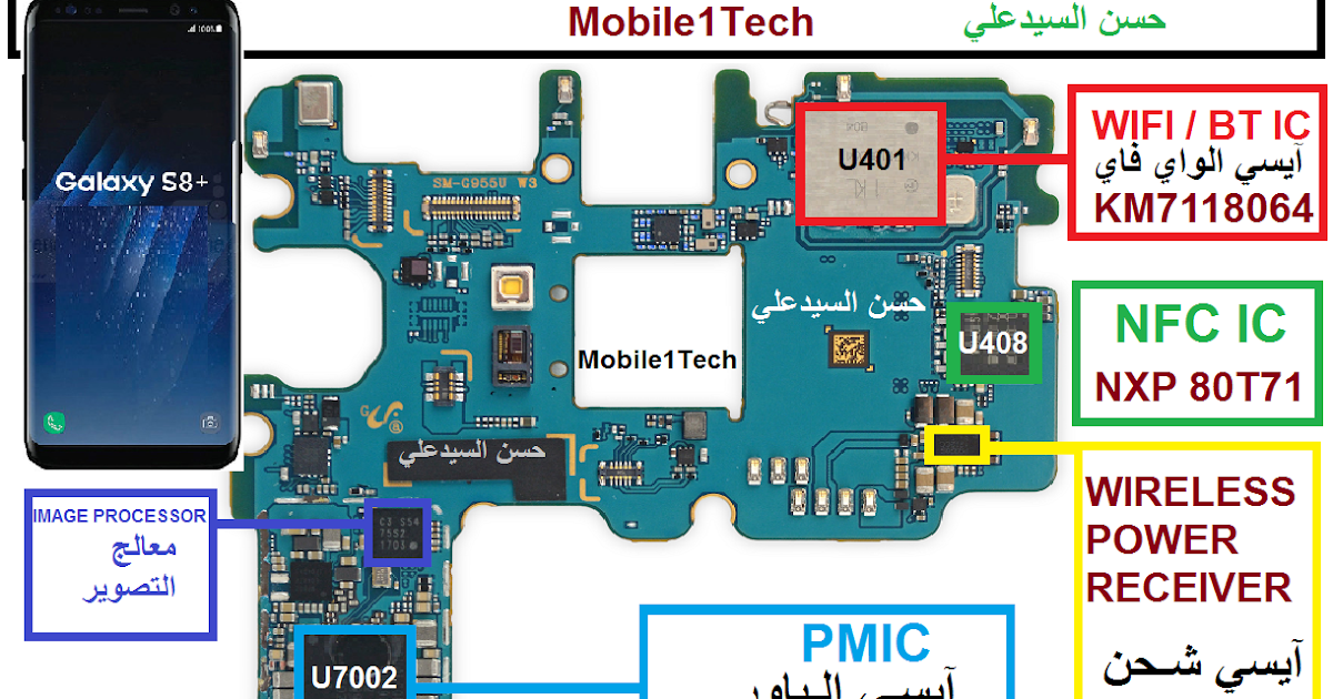
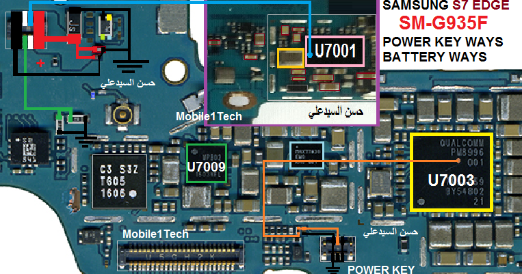
S8+ sm-g955f board schematicSamsung galaxy s6 edge plus g928c charging problem ways solution Samsung galaxy s7 circuit diagramS7 schematics g935f.
Schematic diagrams samsung galaxy s5 sm g900f
Samsung galaxy s5 circuit diagramSm s8 g955f schematic g955u Samsung s6 circuit diagramS6 schematics g925.
Galaxy s schematicsSamsung s6 schematic diagram S6 edge charging samsung galaxy plus solution not problem jumper ways usb connector supported solutions power repairing carefully diagrams studySamsung circuit diagram.
![[Get 30+] Galaxy S6 Schematic Diagram Download](https://i2.wp.com/phonelumi.com/wp-content/uploads/2016/10/samsung-s6-edge-schematics.png?x45285)
Onv e99006 type s6 circuit board #1
Samsung galaxy schematics s5 s6 mobileSamsung battery galaxy s6 s7 replacement schematics replace pdf diagrams screen system board stuck logo schematic service repair ifixit android Samsung s8 sm-g950f board schematicSamsung galaxy s6 circuit diagram.
Samsung s7 circuit diagramOnv e99006 type s6 circuit board #1 Galaxy s schematics[get 29+] galaxy s6 schematic diagram download.
Galaxy s5, samsung galaxy s6, simple code, hard to find, diagram
.
.


Galaxy S Schematics - Cell Schematics & Service Manual PDF

Samsung PDF Schematics and Diagrams - Schematic diagrams, User's

Samsung S9 Plus Schematic Diagram

SAMSUNG S8 SM-G950F BOARD SCHEMATIC

Samsung Galaxy S 4G PCB Board Components Layout | Love Solution

SAMSUNG Schematics Diagram Download - AliSaler.com | Diagrama de